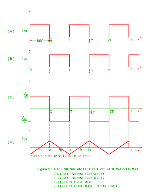
Effect of type of Load on output waveform
Resistive load
- The load voltage and
load current waveform do not have any phase displacement when the resistive
load is connected at the output.
R – L load
The working of the
single phase half bridge inverter is explain as follows
Mode 1 ( t1
< t < t2 )
- The load receives Vdc
/ 2 voltage when the SCR T1 is turned on and load current increases
slowly and exponentially.
- The load voltage and load current polarity becomes
equal when SCR T1 is turned off. The energy stored in the load during this
interval.
Mode 2 ( t2
< t < t3 )
- The flow of inductive load
current continues to flow when SCR T1 is turned off.
- The direction of load
voltage reverses.
- The load current flows through conduction of lower half diode
D2. The stored energy of load feedback to lower half.
Mode 3 ( t3
< t < t4 )
- The load current
becomes zero and SCR T2 is turned on during this interval.
- The voltage across
load becomes – Vdc / 2.
- The
load current becomes maximum negative at the end of this period ( t4
time ).
Mode 4 ( t4
< t < t5 )
- The SCR T2 is turned
off at time t4 but the load current continues to flow due to
inductive load.
- The voltage across load becomes equal to + Vdc / 2.
- The load current flows through upper half portion due to conduction of diode D1.
- The energy stored of load feedback to upper part of the supply source.
- The power flows from
supply to load and vice versa.
- The main disadvantage of the single phase half
bridge inverter is that it requires three wire DC supplies.


