Introduction
- The commutation circuit of SCR is costly in order to turn off in the DC circuit.
- The main disadvantage of the GTO is that it requires very high negative current in order to turns it off.
- ( If the anode current of the SCR is 100 amp, the negative gate current requires to turn off the GTO should be 20 to 25 amp ).
Negative gate current = Anode current / Turn off
current gain
- The power MOSFET is used for low voltage and low power application because of high input impedance, higher switching speed, simple control circuit, low current density and higher forward voltage drop.
- The IGBT and MCT are semiconductor devices which combines characteristics of both BJT and FET.
- The characteristic of the IGBT is much superior to the BJT whereas the characteristic of MCT is superior to the SCR.
- The MOSFET in the MCT is used to turn on and turn off the device.
- The MCT consists of two MOSFET, one MOSFET is used to turn on the device and other MOSFET is used to turn off the device.
Symbol and Equivalent Circuit
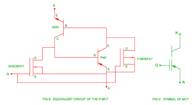
- The symbol of MCT is shown in the Figure.
- It has three terminals anode, cathode and gate.
- The equivalent circuit of MCT consists of two transistors and two MOSFET.
- The P channel MOSFET is connected between collector and emitter terminal of PNP transistor whereas N channel transistor is connected between emitter and base terminal of PNP transistor.
- The P channel MOSFET is associated with turn on process whereas N channel MOSFET is associated with turn off process.
Structure
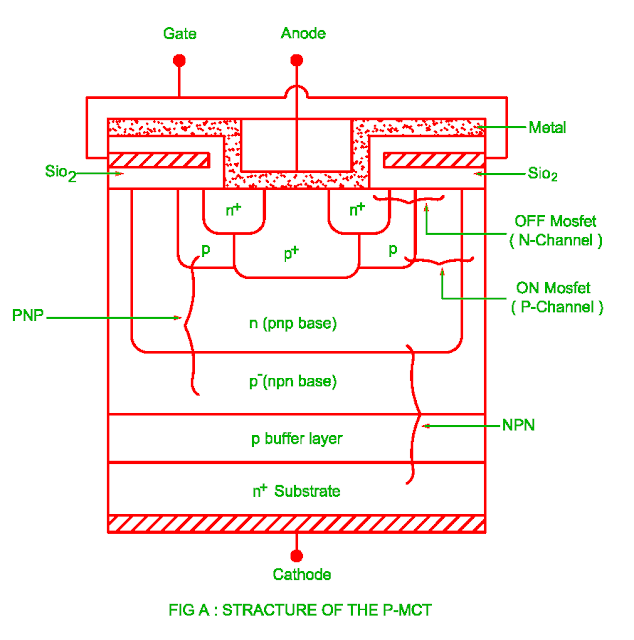
- The single cell structure of the P – MCT is shown in the figure A.
- There are thousands of cell connected in parallel in order to increase current capacity and its fabrication is done on single silicon wafer. The P buffer layer lies between P- base layer and n+ substrate layer in the punch through MCT ( P – MCT ).
- There is no P type buffer layer in the non – punch through MCT.
- The single cell MCT consists of one SCR and two MOSFET. One MOSFET is used to switch on the device whereas the other MOSFET is used to switch off the device.
- The P channel MOSFET is connected between collector and emitter of the PNP transistor and N channel MOSFET is connected between base and emitter of the PNP transistor.
- The P channel MOSFET is used to turn on the device whereas the N channel MOSFET is used to turn off the device.
- The MCT is called as complementary MCT because the gate is made negative with respect to anode instead of the cathode.
Turn on process
- The gate is made positive with respect to anode to turn off the device.
- When the gate is made negative with respect to anode, the P - MOSFET is turned on therefore drain current flows through the base of the NPN transistor resulting it turns on.
- The collector of the NPN transistor is connected to the base of the PNP transistor resulting it turns on.
- Therefore the MCT is switched on. It remains in ON condition in spite of removing gate pulse.
- The conductivity of the PNP transistor is high as compared to P channel MOSFET therefore the most of the current flows through PNP transistor.
- The N channel MOSFET remains off during this period.
Turn off process
- When the gate is made positive with respect to anode, the N channel MOSFET is switched on.
- This MOSFET is in parallel with base – emitter of the PNP transistor resulting the base current decreases and the MCT is turned off in the short time.
- The current gain of the PNP transistor is high, it is connected with parallel to N channel MOSFET.
- All cells of MCT must be turned off at a time in order to turn off MCT otherwise high current density of the one cell may damage the device.
- The drain – source voltage of the device is less than 0.7 voltage in order to turn off the device
Static Characteristics
- The static characteristic of the MCT is similar to that of the SCR and GTO.
- The MCT has low reverse breaking capability ( 20 - 30 V ).
- The ON state voltage drop of the MCT is greater than the SCR but less than GTO.
Features
- High switching speed due to two MOSFET (1 Micro second )
- Temp co-efficient low at negative current and high at positive current
- Low on state voltage drop ( 1.1 volt )
- Simple Gate drive circuit due to high input impedance
- Low switching power loss
- MCT is connected in parallel when high power is required
- High current density as compared to IGBT
You may also like :


